
AcSiP has provided engineering service to help clients in RF module design into their IoT projects.
There are rich resources for technical specific support purpose.
|
|


Developer could ask AcSiP salesperson for items consulted and first article inspection support or leave message through following form as well.
|
|
.png)
| 。Schematic review |
| 。RF layout check and switch control |
| 。RF measuring and field test, deployment |
| 。Antenna matching |
| 。Certification test items, materials |
| 。SDK, firmware, LPWAN protocol |
| 。Pre-set configuration in FW |
| 。Customize demands |
For example, there are common consulted cases show below.
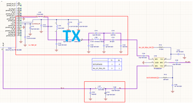
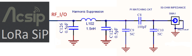
RF Matching and Control
RF impedance control and matching optimization, which greatly saves the time required to manually adjust the matching value of the product.
|
|
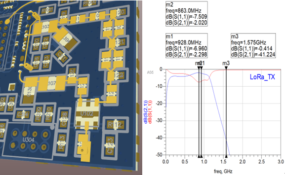
PCB Antenna Simulation
Epoxy resin use as printed antenna radome has effected antenna performance on the electromagnetic wave propagation.
|
|
.png)
Essential information in Application Note file
Developer of product in PCB design while integrated AcSiP RF module need to checkout reminding note about RF design knowledge in Application Node of product.There are description about layout guide there for reference.
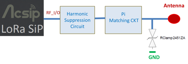
- ESD Protection and Harmonic suppression
|
|
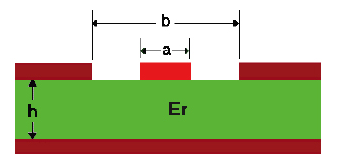
- RF Trace Management
CPWG model is recommended for RF trace calculation, which has better EMC and RF capability. And please discuss with PCB manufacturer to evaluate and keep RF trace in 50ohm.
The values of a and b will affect each other, it is best to control it not to be too wide from the width and gap of the output pad of the module.
|
|
For more information, or for sales inquiries, please contact AcSiP Technology Corp.